RFID is most arguably a evolutionary wireless technology which boosted working of embedded devices up to great mark. And there is plenty of systems and devices working based on this technology. This article is focused to teach you how to interface RFID with AVR microcontroller. Before moving on to that interfacing part let’s begin with what RFID exactly is and how it works?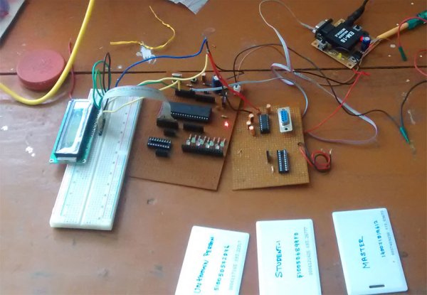
Radio Frequency identification describes the system in which the identity of an individual or object is transmitted by means of a unique serial number through radio waves. Usually RFID system consists of two basic components they are
- Tag
- Reader
RFID tags consists of a simple Microchip which stores 12 byte unique ID and an antenna through which the unique ID is read by the reader. Whereas Reader is nothing but a specifically designed hardware module that senses the tag whenever it brought within a specific range say for example 10cms. The reader emit radio waves and receive signals back from the tag which comes with different operating frequency and sensing distance.
When a RFID tag is brought within the specific range of the reader the unique ID is sensed. After reading the ID from the tag is read by the reader and then that unique id is passed onto a controller/processor. The controller in turn performs specific action using that ID based on the written code
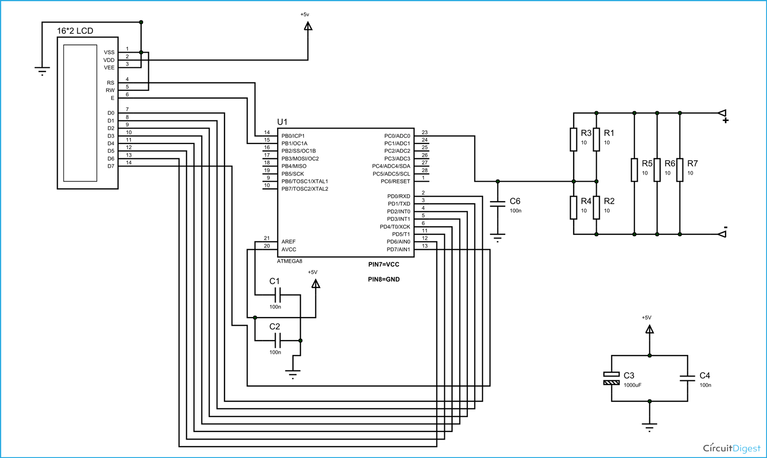
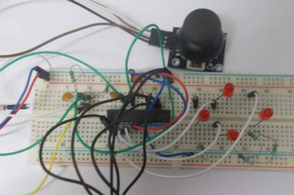
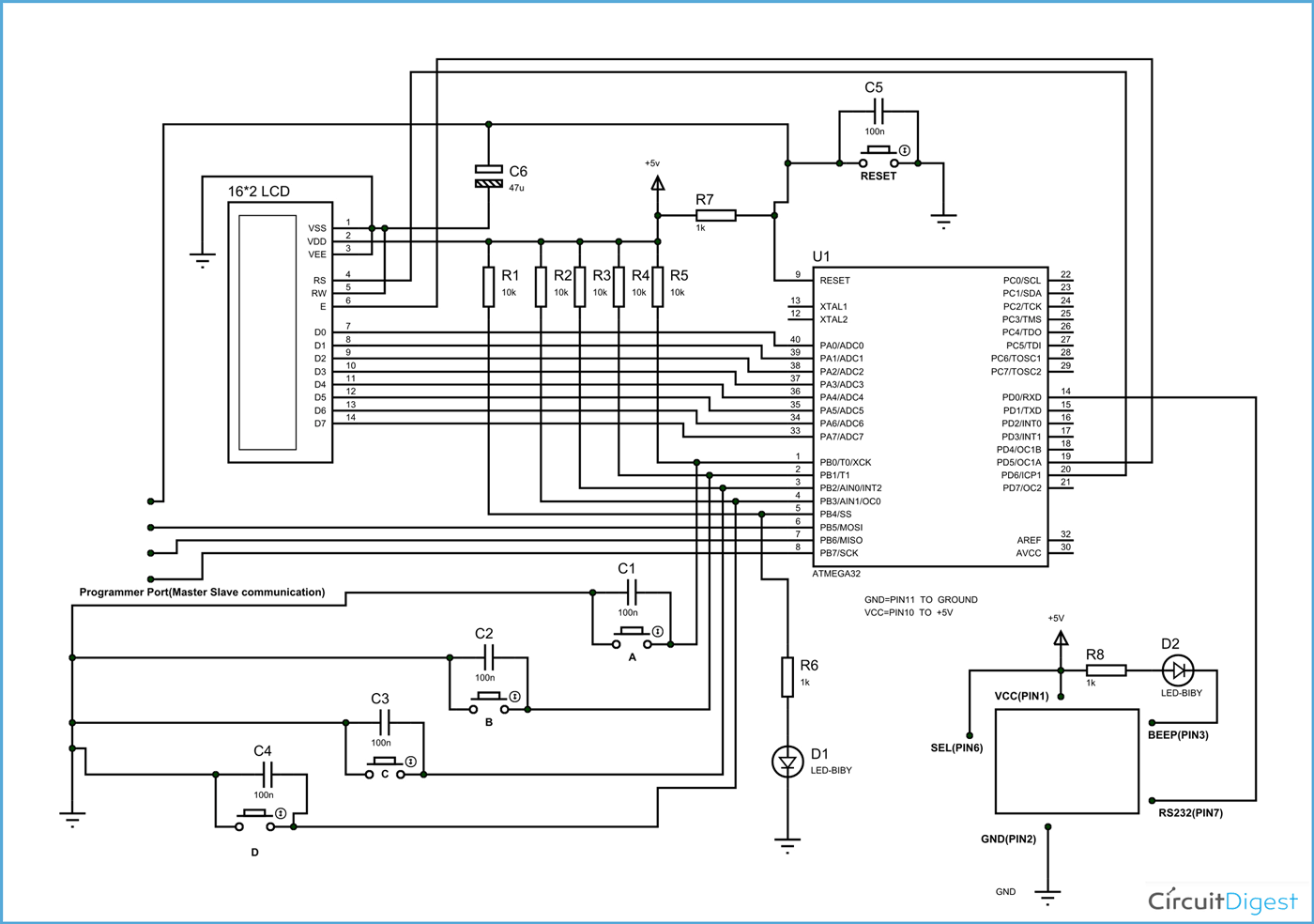
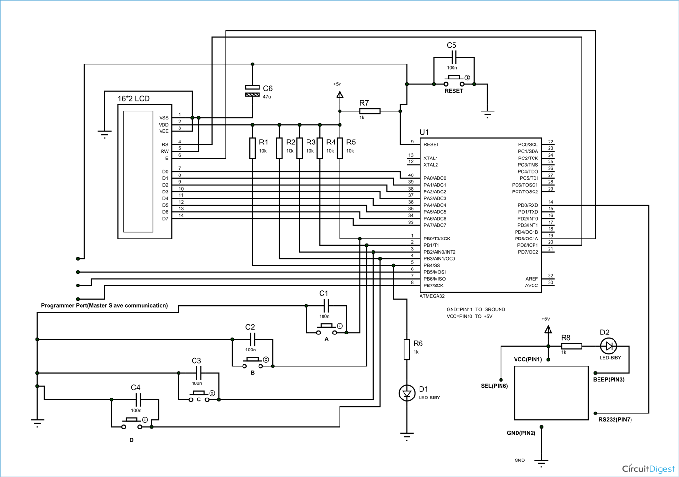
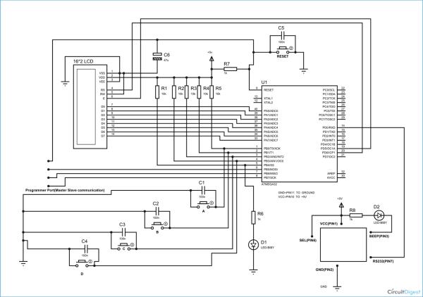
SCHEMATIC DESIGN OF RFID INTERFACE WITH AVR:![Schematic How to interface RFID with AVR ATmega32 microcontroller]()
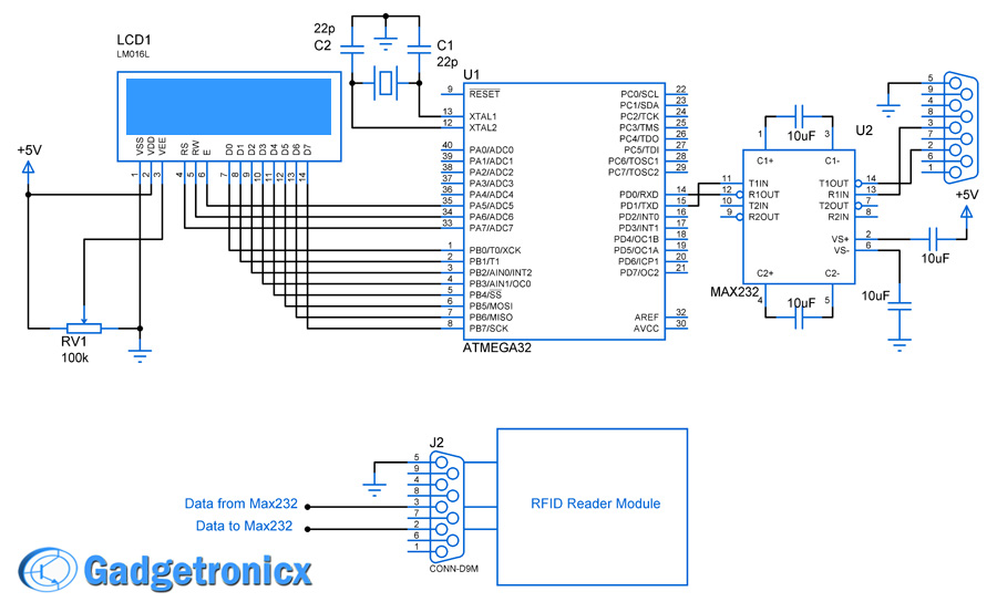
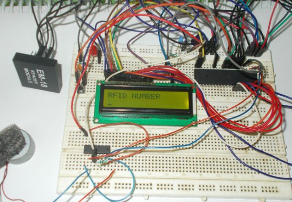
RFID module works at RS232 logic levels hence ATmega32 is connected to RFID module by means of a level converter IC MAX232. The unique ID from the RFID tag is converted into serial mode by means of the reader module and then transmitted to controller via MAX232. The baud rate is set to 9600bps for data transmission. The code was written in such a way when a card/tag comes in the proximity of RFID reader, the microcontroller reads the code and sends it to the LCD module for displaying
For more detail: How to interface RFID with AVR ATmega32 microcontroller