Quantcast
Channel: AVR ATmega Projects Archives - Projects Tutorials Code Library for Atmels Atmega32 AVR
Viewing all 1082 articles
Browse latest View live

DSPIC33FJ128GP NOKIA 6100 LCD DRIVER CIRCUIT ATMEGA168

$
0
0


@ Erhan brother Atmega8 prepared with the application had shared (Atmel Atmega8 Nokia 6100 LCD (pcf8833) application) I In addition to the helpful one more example’ll share the codes and microchip dspıc33fj128gp both the… Electronics Projects, dsPIC33FJ128GP Nokia 6100 LCD driver circuit ATmega168 “avr project, dspic projects, microcontroller projects, “

NOKIA 6100 LCD DRIVER CIRCUIT

@ Erhan brother Atmega8 prepared with the application had shared (Atmel Atmega8 Nokia 6100 LCD (pcf8833) application) I In addition to the helpful one more example’ll share the codes and microchip dspıc33fj128gp both the Atmel ATmega168 microcontroller can be used with.

Nokia 6100 test circuit image;

NOKIA 6100 LCD DRIVER CIRCUIT (1)

NOKIA 6100 LCD DRIVER CIRCUIT

Written by Dan Stahlke, dstahlke@gmail.com, http://www.stahlke.org/dan/nokialcd The driver was based upon an example written by SparkFun, and the font was taken from the KS0108 library (http://en.radzio.dxp.pl) and is (c) Rados³aw Kwiecieñ, radek@dxp.pl This code can be used for any purpose, free or commercial, but there is no warranty implied whatsoever.

This package contains drivers for the Nokia 6100 LCD. The driver has only been tested with the new Epson unit from SparkFun (Chinese clone, red tab on protective cover, green PCB with brown traces). It should work with the Philips or the older Epson chips too but will inevitably need some fixes (in particular the LCD_Y_OFFSET variable should probably be set to zero). If you get it to work with other chipsets please let me know. You may also have to edit the contrast setting which is defined in the LCDInitController function

This code has been tested with the ATmega168 and dsPIC33FJ128GP chips, and makefiles are included for each. The makefiles are a bit Linux-centric and may need some editing. Alternatively, you could easily bring this code into the Microchip or Atmel IDE. In this case you must make sure to pass the “-DEPSON” or “-DPHILIPS” flag to the C compiler to tell the code which LCD chipset you are using.

If you want to port this code to a new MCU all you need to do is provide code to initialize the ports and to do a 9-bit SPI transfer. Look in the sysconfig-*.c files for examples.

The graphics routines you get basically consist of functions for setting individual pixels, filling rectangles, drawing text, and drawing raster blocks. There is no code for diagonal lines or circles (when is the last time you have actually seen this functionality used on an LCD?). Feel free to add more routines and send me patches. The code in demo_testpattern.c is probably a good way to learn how to use this driver.

See the end of this file for a wiring diagram. You don’t really need to use the MISO pin. This is used for reading from the display, which is not currently implemented. If you leave this out make sure to keep the 1k resistor between MOSI and the LCD DIO pin. The DIO pin is both an input and an output, and the resistor provides safety in the case where both the LCD and the MCU are outputting at the same time.


CNC PROJECT ATMEGA16 X-Y-Z MOTOR CONTROL CIRCUIT

$
0
0

ATMega16 microcontroller based on a detailed cnc project with computer com RS232 on port communicating project’s source C code, schematics eagle CAM (graphic printout is used to direct the CNC circuitry and sent to)… Electronics Projects, CNC Project ATMega16 X-Y-Z Motor Control Circuit “avr project, microcontroller projects, “

MOTOR CONTROL CIRCUIT

ATMega16 microcontroller based on a detailed cnc project with computer com RS232 on port communicating project’s source C code, schematics eagle CAM (graphic printout is used to direct the CNC circuitry and sent to) files bulunuyorayrı mechanic parts of 3-d images were shared. Test video with a simple picture drawn on the CNC. Motor Control Circuit

MOTOR CONTROL CIRCUIT (1) MOTOR CONTROL CIRCUIT (2) MOTOR CONTROL CIRCUIT (3) MOTOR CONTROL CIRCUIT (4) MOTOR CONTROL CIRCUIT (5) MOTOR CONTROL CIRCUIT (6) MOTOR CONTROL CIRCUIT (7) MOTOR CONTROL CIRCUIT (8) MOTOR CONTROL CIRCUIT (9)

Source: https://320volt.com/en/atmega16-cnc-projesi-x-y-z-motor-kontrol/ Alternative link: cnc-project-atmega16-x-y-z-motor-control-circuit.rar

How to build alarm security system using motion sensor with PCB Prototyping

$
0
0


Introduction

Security is important for everyone from our homes to places of work. You need to feel safe when you are sleeping at night. You might have important documents that you need to keep private. Sometimes you have property in your house that must be secured. Well, you need a good security system. This way you can leave the house and travel for your holidays without having to worry about break-ins. Intruders will stay way from your home when you have a perfect alarm security system. This security system is one that you can get the hardware components at your local store. You will be able to design it yourself after I take you step by step on how to do it.  I will take you through steps on how to make a security with motion detection. The instructions will be clear and straight to the point to ease your work.  The components are pocket friendly and will not cost you a fortune. Value for your money is considered while you help yourself to a secure place. The PCB assembly will entail a number of tools and materials. We will use the PIR sensor and Arduino to come up with an alarm security system.  With a motion sensor you can have the chance of doing something before things take a turn. For instance, when there is an intruder and the alarm goes on, you will alert the authorities. Safety is paramount to you and your family.

Arduino is being used in this project as its a complete board built using AVR microcontroller family. Easy to build project, with hundred of library code samples and much more.

Materials needed

  • Speaker
  • Arduino Uno
  • LED of your choice
  • Assorted wire
  • PCB board
  • A parallax PIR motion sensor
  • Plastic card box
  • Zip ties
  • Spray paint
  • A Solder

Tools required include;

  • A Soldering iron
  • A Computer and also Arduino USB cable
  • A drill
  • A saw
  • Wire strippers
build alarm security system using motion sensor with PCB Prototyping

Tools and materials

Procedure

1.Assembling the PIR Sensor

The first step is to assemble the motion sensor. You will need to open the sensor and Printed Circuit Board (PCB). After opening the two materials you can then proceed to position the three pins that are in the sensor on to the Printed Circuit Board. After positioning it on the row at the front, you can now solder it directly to the board. The board that you will solder is the one with the metallic pads, not the blank one

After soldering the parts you will then examine the pins. You should be keen so that you can properly have the pins. They should read as VCC, GND, and OUT. Later you will use the VCC to plug in the +5V. The GND will proceed to the ground and as for the OUT, it will go to the digital pin meant for the Arduino.

Then you have to solder three wires just behind where you had soldered the three pins before. This means that on the board bottom you will have a total of 6 solder points. You have to do this right so that at the end you have the correct alarm security system. You can now connect each pin to the solder points. Depending on the position of the sensor that you need, ensure that the wires are long enough.

PCB Board

PCB Board

PIR motion sensor

PIR motion sensor

2. Setting up the Arduino

This will be a simple task that will take a short time.  It will require you to first connect the GND wire of the PIR sensor that goes to the ground to the Arduino. The next step is to also connect the VCC on the sensor to the Arduino. Finally connect the OUT from the sensor to pin #7 on the Arduino as well. The instructions here are simple and precise to follow.

By now you need to get the LED and the speaker so as to fix it on the Arduino. For the speaker you can go ahead and connect the + to pin #9 of the Arduino. You can then connect – of the speaker to the ground of the Arduino. The LED is the next connection whereby you will fix the long leg to pin #13 of the Arduino. You can also get the short leg of the LED and connect it to the ground of Arduino. The ground is next to pin#13 hence it will not be a challenge to find.

At this time the end result will tell you if you did the PCB SMT well. Upload the sketch to the board that you have and then plug the Arduino in.  You will be able to see some light. If you really connected the PIR sensor to the Arduino in the right way, there will be a buzzing sound.  It will happen even without movement. These two signs will alert that you did the work well. After approximately fifteen seconds, the sensor will then calibrate and the buzzing sound will automatically go off. You will now have a functional security system at this point. The finished product will be able to sense any movements around your place of residence or your work place.

Arduino

Arduino

3. Finalising the system

With a plastic card box and paint the end product will be even better. Using the card box cut all the holes so that the wires are let out. You can ensure that everything else is well tucked in. The holes will be one at the back for the wires to the speaker and also the sensor. The second hole at the top will serve the LED. The last hole at the front will be for the USB cable that powers the Arduino.

The spray paint will come in handy now. You can choose the colour you like as per your taste and preference. The enclosure box will then be appealing after you have done an excellent painting. The alarm system will now be ready for use.  The alarm will be triggered whenever there is any motion and you can check it out. A feeling of satisfaction will engulf you as you see the work of your hands.build alarm security system using motion sensor with PCB Prototyping

Conclusion

This PCB project is simple and easy to follow. You will not go wrong when you follow the steps keenly. As I had earlier said, the hardware components are available in the market. The best part is that you can customize the end product how you like it. I hope this inspires you to create your own alarm security system. If you are interested, I can sponsor you the PCB board. You can be sure that I will send one to you. We can make arrangements on how best you can purchase the equipment. You can go ahead and reach put to me through my website link.

Thanks for PCB prototype manufacture PCBGOGO to sponsor me this project.

If you like it, please share it and you also can buy some nice PCB form them.

ELECTRONIC PIANO CIRCUIT ATTINY2313 SIMPLE AUDIO PROJECT

$
0
0

Atmel ATtiny2313 two 1.5V AA batteries powered electronic piano circuit connected in series (3V) can be operated. PB3 – PB4 16 on pins 15 and 32 ohm speaker connected to these pins as exit…. Electronics Projects, Electronic Piano Circuit Attiny2313 Simple Audio Project “avr project, microcontroller projects, “

ELECTRONIC PIANO CIRCUIT

Atmel ATtiny2313 two 1.5V AA batteries powered electronic piano circuit connected in series (3V) can be operated. PB3 – PB4 16 on pins 15 and 32 ohm speaker connected to these pins as exit. 13 pieces in varying shades of sound produced by this tone. AVR programming beginners a good example for people.

ELECTRONIC PIANO CIRCUIT schamatic

Source: https://320volt.com/en/attiny2313-basit-ses-devresi-elektronik-piyano-c-dili/ Alternative link: electronic-piano-circuit-attiny2313-simple-audio-project.zip

STAR LED EFFECTS CIRCUIT ATTINY13 PROJECT

$
0
0

Stars in the shape of hard work to prepare printed circuit board design for SMD LEDs to be mounted like a great deal of attention and effort, but finally emerged quite nice circuit noncontiguous… Electronics Projects, Star LED Effects Circuit ATTINY13 Project “avr project, led projects, microcontroller projects, “

STAR LED EFFECTS CIRCUIT

Stars in the shape of hard work to prepare printed circuit board design for SMD LEDs to be mounted like a great deal of attention and effort, but finally emerged quite nice circuit noncontiguous clusters of LEDs flashing creates a beautiful image. 114 pcs SMD LED effects used in the circuit.

ATTINY13 eagle printed circuit control board regulations drawn with different shapes can be achieved by making the source code files have bascom.

STAR LED EFFECTS CIRCUIT (1) STAR LED EFFECTS CIRCUIT (2) STAR LED EFFECTS CIRCUIT (3)

Source https://320volt.com/en/attiny13-yildiz-seklinde-smd-ledli-efekt-devresi/ Alternative link: star-led-effects-circuit-attiny13-project.rar

ACTIVE ELECTRONIC LOAD CIRCUIT ATMEGA88 100W DUMMY LOAD

$
0
0

In each electronic device in one form or another there is a power supply unit (PSU). Of course, because no one will work for free. Before connecting to the circuit, it would be nice to see how the PSU works at different loads.

Personally, I am not inspired by the search for a set of different-sized resistances with subsequent testing of the power supply with each of them; it is much more convenient to make a “load” that can be smoothly adjusted.

ACTIVE ELECTRONIC LOAD CIRCUIT

What did you want

So what did I want to get as a result?

  • Current consumption 0-5A (enough almost everywhere)
  • Power consumption – up to 100W (enough for almost any power supply)
  • Maximum voltage – 200V
  • Current indication
  • Mode when the load is periodically turned on and off ( for testing and setting feedback )

Housing

The body (like almost all the other parts), I pulled out of the old stock. Yes, I bought only an indicator and M2.5 screws for it, the rest I already had.

The case from some old switch LPT ports of ancient times, the giblets were pulled out and put to the trash can.

Cutting out the holes for the indicator and for the fan was absolutely epic, because the body is made of mercilessly thick steel.

Stalyuk I cut Dremel, and here’s what I can say:

  1. Self-made cutting discs for Dremel from grinders are absolutely steering.
  2. It is necessary to cut thick metal with a disk standing at 45 degrees to the metal plane, then the cut is smooth.

I cut such a huge hole, and not just drilled a dozen small holes because the power transistor did not have enough body height.

The photo shows how it happened. Taking into account the fact that this is a handwork, it turned out pretty well.

ACTIVE ELECTRONIC LOAD CIRCUIT (1)

Electronics

Active load electronics are as simple as boots. You can see the scheme here:

There is nothing fundamentally new there for you.

ACTIVE ELECTRONIC LOAD CIRCUIT (2)

Highlights:

  • What surprised me is that there are very specific datasheets for computer fans. In the diagram, the FanPower leg turns on the fan. At the same time it starts spinning at minimum speed. Theoretically, it is possible to start PWM on the FanSpeed foot and control the fan smoothly. But I just turn it on or off.Three stages will turn out: Off, low speed, high speed.
  • Current adjustment is assembled as a divider on resistors R5, R18 and resistors R20 and R21 (in gray square.)
  • The current switch is quite exotic (it was stuck when the board was ready) – when the DisableCurrent leg is in the input mode on the microcontroller, the U6 U op-amp normally controls the current of the power transistor. When the controller wants to turn off the current, it puts this foot in a high state. OU ofigevat from, as it seems to him, a huge current through the power transistor, and quickly closes it.
  • As a protective (reversal) diode, I found the BYV32E-200. Quite an interesting diode – physically it is a normal pn diode, but its fall is more like a Schottky diode.

Soft

Software is my attempt to lose with C ++ on microcontrollers. On the one hand, it turned out to be interesting, on the other hand, there are a lot of places in the pros where they just make me furious.Firmware for AVR under IAR. It turned out, as always when trying to play, crooked.

In any case, the advantages for microcontrollers are the topic of a separate article.

Files

Download all the documentation here (there is also a hex):

http://hg.bsvi.ru/active-load

What happened

This work weighs quite well, and causes a sensation of a well-made device. One hundred watts dissipates, though with decent heating (And no one said it would be easy).

Some of the parameters did not turn out the way they wanted, but they’re too lazy to redo them, moreover, they are not too critical for me. For example, the turn-on time is 80µS. This is not exactly a delta pulse, and the feedback cannot show the transition process in all its glory. On the other hand, frankly I get on in OS it will help to reveal.

ACTIVE ELECTRONIC LOAD CIRCUIT (3)

Vidushnik with a demonstration

Yes, yes, I myself know that the quality is terrible and it is time to buy a new camera. I am now in her active selection. I don’t know what to do with my congenital inhibition, but I hope I’ll fix it))

Protel pcb project’s source code and have the schema files, IAR.

Source: http://bsvi.ru/aktivnaya-nagruzka/alternative active-electronic-load-circuit-atmega88-100w-dummy-load.rar

220V SOLDERING IRON TEMPERATURE CONTROL WITH AT89C2051 LED DISPLAY

$
0
0

Sold in the market potency heat settings with TRIAC 220v temperature-controlled soldering iron more advanced version control AT89C2051 microcontroller is provided by heat setting 2 button is made with indicators, one for led display… Electronics Projects, 220V Soldering Iron Temperature Control with AT89C2051 LED Display “avr project, microcontroller projects, “

IRON TEMPERATURE CONTROL

Sold in the market potency heat settings with TRIAC 220v temperature-controlled soldering iron more advanced version control AT89C2051 microcontroller is provided by heat setting 2 button is made with indicators, one for led display used temperature% are read.

Control circuit with triac driver moc3041 opto-isolated circuit diagram Triac T he G Gheit stated as the cathode and the anode K can use triac BT138. Source C code given to the project.

DIGITAL SOLDERING STATION CIRCUIT

IRON TEMPERATURE CONTROL (1)

Source: http://ahtoxa.net/micros/at89c2051/power-reg/ Alternative link: 220v-soldering-iron-temperature-control-with-at89c2051-led-display.rar

ATMEGA8 BIPOLAR STEPPER MOTOR DRIVER CIRCUIT L293B

$
0
0

Bipolar stepper motor control circuit 6v … 35v inter able to run power 1 amp on the circuit control, program, sensor, PWM, UART has links ATMega8 output used in motor drive l293b circuit of… Electronics Projects,ATMega8 Bipolar Stepper Motor Driver Circuit L293B “atmega8 projects, avr project, microcontroller projects, motor control circuit, motor driver circuit, “

STEPPER MOTOR DRIVER CIRCUIT

Bipolar stepper motor control circuit 6v … 35v inter able to run power 1 amp on the circuit control, program, sensor, PWM, UART has links ATMega8 output used in motor drive l293b circuit of the source c code ares pcb and isis simulation files there. control circuit microcontroller atmel atmega8 motor control L293

BIPOLAR STEPPER MOTOR CIRCUIT L293B

STEPPER MOTOR DRIVER CIRCUIT (1)

Source: http://railab.ru L293B ATmega8 step motor control circuit pcb, circuit, code files alternative link: atmega8-bipolar-stepper-motor-driver-circuit-l293b.rar


REMOTE-CONTROLLED DIGITAL TIMER CIRCUIT WITH ATMEL ATTINY2313

$
0
0

Based on Atmel ATtiny2313 microcontroller circuit with the remote control forward / reverse control can be done over time led display are viewing. ATtiny2313 by the time specified number 9 which is connected to…Electronics Projects, Remote-Controlled Digital Timer Circuit with Atmel ATtiny2313 “avr project, microcontroller projects, “

DIGITAL TIMER CIRCUIT

Based on Atmel ATtiny2313 microcontroller circuit with the remote control forward / reverse control can be done over time led display are viewing. ATtiny2313 by the time specified number 9 which is connected to pin PD5 trying to relay is happening.

RC5 protocol used for remote control of the circuit can be used any source control settings sigot c hex codes, pcb, diagrams, dimensions, etc. dry. There are files.

DIGITAL TIMER CIRCUIT REMOTE CONTROL

DIGITAL TIMER CIRCUIT REMOTE CONTROL

Source: https://320volt.com/en/attiny2313-ile-uzaktan-kumandali-dijital-zamanlayici-devresi/ Atmel ATtiny2313 Digital Timer Circuit Alternative link: remote-controlled-digital-timer-circuit-with-atmel-attiny2313.rar

ATMEL ATTINY15 MICROCONTROLLER EXAMPLE DC TO DC CONVERTER CIRCUIT

$
0
0

Atmel ATtiny15 Microcontroller DC to DC converter circuit 3.6 Li-Ion battery voltage of 5 volts raises a more detailed circuit attiny15 not a good example for software power control with microcontroller assembly language prepared… Electronics Projects, Atmel ATtiny15 Microcontroller Example DC to DC Converter Circuit “avr project, dc dc converter circuit, simple circuit projects, “

DC CONVERTER CIRCUIT

Atmel ATtiny15 Microcontroller DC to DC converter circuit 3.6 Li-Ion battery voltage of 5 volts raises a more detailed circuit attiny15 not a good example for software power control with microcontroller assembly language prepared by

ATTiny15: 1 – RESET, 2 – UB/2, 3 – UA/3, 4 – GND, 5 – /SHUTDOWN, 6 – output – PWM, 7 – output – /Enable, 8 – UBatt

DC DC CONVERTER PROJECT SCHEMATIC

DC DC CONVERTER PROJECT SCHEMATIC

Hazırlayan: Joerg Wolfram DC to DC converter circuit, pcb,

source file : https://320volt.com/en/attiny15-ile-dc-dc-konvetor-ornegi-3-6v-5v-assembly/ source assembly code files: atmel-attiny15-microcontroller-example-dc-to-dc-converter-circuit.ZIP

RF TRANSCEIVER EXAMPLE WATER GUN PROJECT CIRCUIT TX434 ATMEGA8 RX434

$
0
0

The RF transceiver with ATmega8 prepared samples prepared with C language software has all the source code for the application circuit used joke 🙂 handmade by remote control a water gun at school students…Electronics Projects, RF Transceiver Example Water Gun Project Circuit TX434 ATMega8 RX434″atmega8 projects, avr project, microcontroller projects, “

WATER GUN PROJECT CIRCUIT

The RF transceiver with ATmega8 prepared samples prepared with C language software has all the source code for the application circuit used joke 🙂 handmade by remote control a water gun at school students have soak 🙂

PET bottles used to store water gun ATMega8 reinforced with 13 mosfet pin number to pop the water tested. TX434 and RX434 RF modules used

WATER GUN PROJECT CIRCUIT (1) WATER GUN PROJECT CIRCUIT (2)

Source: https://320volt.com/en/atmega8-rf-alici-verici-ornegi-tx434-rx434-uzaktan-su-tabancasi-kontrolu/ RF Transceiver ATMega8 Example Water Gun Circuit files alternative link: rf-transceiver-example-water-gun-project-circuit-tx434-atmega8-rx434.RAR

ATMEL APPLICATION NOTES AND SOURCE C ASM CODE

$
0
0

Atmel’s products and practices related to application notes prepared for the asm code source c c language prepared by the majority of the samples. 138’s application List: 1-Register and Bit-Name Definitions for the AVR… Electronics Projects, Atmel application notes and source c asm code “avr project, microcontroller projects, “

ATMEL APPLICATION using Atmage

Atmel’s products and practices related to application notes prepared for the asm code source c c language prepared by the majority of the samples. 138’s application

List:

1-Register and Bit-Name Definitions for the AVR Microcontrollers
2-Accessing the eeprom
3-Block Copy Routines
4-Setup and Use the Analog Comparator
5-Multiply and Divide Routines
6-16-bit Arithmetics
7-BCD Arithmetics
8-Bubble Sort
9-8-point Moving Average Filter
10-Half Duplex Interrupt Driven Software UART
11-Low Cost A/D Converter
12-In-System Programming
13-Half Duplex Compact Software UART
14-8-bit Precision A/D Converter
15-Understanding the AVR ICEPRO I/O Registers
16-External Brown-out Protection
17-Linker Command Files for the IAR ICCA90 Compiler
18-Software SPI Master
19-CRC Check of Program Memory
20-Step Motor Controller
21-Modifying AT90ICEPRO and ATICE10 to Support Emulation of AT90S8535
22-8-bit Microcontroller Multiplexing LED Drive and a 4 x 4 Keypad
23-4 x 4 Keypad – Wake-up on Keypress
24-Setup and Use of the LPM Instruction
25-Mixing C and Assembly Code with IAR Embedded Workbench for AVR
26-Interfacing the PC AT Keyboard
27-Real Time Clock (RTC) using the Asynchronous Timer
28-Long Delay Generation Using the AVR Microcontroller
29-C Code for Interfacing AVR® to AT17LVXXX FPGA Configuration Memories
30-Using the AVR® UART in C
31-Digital Sound Recorder with AVR® and DataFlash®
32-Modification for Rev. B to Rev. C
33-Xmodem CRC Receive Utility for AVR®
34-RC5 IR Remote Control Receiver
35-Getting Started with IAR Embedded Workbench for Atmel AVR
36-Accessing 16-bit I/O Registers
37-Efficient C Coding for AVR
38-EMC Design Considerations
39-Getting Started with ImageCraft C for AVR
40-Using the AVR® Hardware Multiplier
41-Software LIN Slave
42-Self Programming
43-Battery Charger for SLA, NiCd, NiMH and Li-Ion Batteries
44-Accessing an I2C LCD Display using the AVR® 2-wire Serial Interface
45-DTMF Generator
46-Embedded Web Server
47-Upgrading AT90ICEPRO to ATICE10
48-Quick Start Guide for the Embedded Internet Toolkit
49-Getting Started with the CodeVision AVR C Compiler
50-Replacing ATmega103 by ATmega128
51-Setup and Use the AVR® Timers
52-High-speed Interface to Host EPP Parallel Port
53-Zero Cross Detector
54-Reducing the Power Consumption of the AT90EIT1 – AVR Embedded Internet Toolkit
55-Replacing AT90S4433 by ATmega8
56-Replacing ATmega161 by ATmega162
57-Replacing ATmega163 by ATmega16
58-Replacing ATmega323 by ATmega32
59-Replacing AT90S8515 by ATmega8515
60-Replacing AT90S8535 by ATmega8535
61-AVR Hardware Design Considerations
62-JTAG ICE Communication Protocol
63-STK500 Communication Protocol
64-High Endurance EEPROM Storage
65-Digital Filters with AVR
66-STK502 – A Temperature Monitoring System with LCD Output
67-LCD Driver for the STK502 and AVR Butterfly Matrix Keyboard Decoder
68-RC5 IR Remote Control Transmitter
69-Migrating between ATmega8515 and ATmega162
70-Migrating between ATmega8535 and ATmega16
71-Migrating between ATmega16 and ATmega32
72-Migrating between ATmega64 and ATmega128
73-Buffered Interrupt Controlled EEPROM Writes
74-DES Bootloader
75-Using the AVR’s High-speed PWM
76-Power Efficient High Endurance Parameter Storage in Flash Memory
77-AVR UART as ANSI Terminal Interface
78-Conditional Assembly and portability macros
79-Using the Enhanced Watchdog Timer
80-Replacing ATmega8 by ATmega88
81-Migrating between ATmega48, ATmega88 and ATmega168
82-Calibration of the internal RC oscillator
83-Software Universal Serial Bus (USB)
84-SPI-UART Gateway
85-Characterization and Calibration of the ADC on an AVR
86-Using the USI module as a I2C slave
87-Using the USI module as a I2C master
88-Run-time calibration of
89-the internal RC oscillator
90-Using the TWI module as I2C master
91-Using the TWI module as I2C slave
92-Single-Phase Power/Energy Meter with Tamper Detection
93-AVR Open Source Programmer
94-Direct driving of LCD display using general IO
95-ADPCM Decoder
96-Replacing AT90S4433 by ATmega48
97-C functions for reading and writing to Flash memory
98-Migration between ATmega64 and ATmega645
99-Using the Master SPI Mode of the USART module
100-Using the EEPROM Programming Modes
101-Dallas 1-Wire® master
102-Migration between ATmega169(P) and ATmega329
103-Migration between ATmega128 and ATmega1281/ATmega2561
104-Using the USI module for SPI communication
105-SMbus Slave Using the TWI Module
106-Migration between ATmega165(P) and ATmega325(P)
107-Setup And Use of The SPI
108-JTAGICE mkII Communication Protocol
109-AES Bootloader
110-Replacing ATtiny15 with ATtiny25
111-STK500 Communication Protocol
112-Control of High Voltage 3-Phase BLDC Motor
113-Replacing AT90S/LS2323 or AT90S/LS2343 with ATtiny25
114-Interfacing AVR serial memories
115-Sensorbased control of three phase Brushless DC motor
116-Smart Battery Reference Design
117-Replacing ATtiny11/12 by ATtiny13
118-Replacing AT90S2313 by ATtiny2313
119-Replacing AT90S1200 by ATtiny2313
120-Half Duplex UART Using the USI Module
121-Migrating from ATmega128 to AT90CAN128
122-Brushless DC Motor Control using AT90PWM3 AC Induction Motor Control Using the constant V/f Principle and a Natural PWM Algorithm
123-AC Induction Motor Control Using the Constant V/f Principle and a Space-vector PWM Algorithm
124-LIN v1.3 Protocol Implementation on Atmel AVR Microcontrollers
125-USB Generic HID Implementation
126-USB Keyboard Demonstration
127-USB Firmware Architecture
128-USB Mouse Demonstration
129-Migration between ATmega16/32 and ATmega164P/324P/644(P)
130-Using a 32kHz XTAL for run-time calibration of the internal RC
131-Enhancing ADC resolution by oversampling
132-Intelligent BLDC Fan Controller with Temperature Sensor and Serial Interface
133-PC Fan Control using ATtiny13
134-Sensorless Control of Two-Phase Brushless DC Motor
135-Sensorless control of 3-phase brushless DC motors
136-Code Lock with 4×4 Keypad and I2C™ LCD
137-Using Timer Capture to Measure PWM Duty Cycle
138-AVRISP mkII Communication Protocol

Download All the files the Atmel avr applications:http://www.mediafire.com/file/hyz81n960tfkde4/atmel-uygulama-notlari-ve-kaynak-c-asm-kodlari.rar

ADC EXAMPLE ATMEGA8 DIGITAL VOLT METER AMMETER AVR PROJECT

$
0
0

ADC – analog-to-digital converter (ADC-Analog-to-Digital Converter). Converts a certain analog signal to digital. Bitrate ADC determines the accuracy of the signal conversion. Conversion time – respectively, the speed of the ADC. The ADC is embedded in many microcontrollers of the AVR family and simplifies the use of the microcontroller in any regulation schemes where it is necessary to digitize a certain analog signal.
Consider the principle of operation of the ADC . To convert, you need a reference voltage source and the actual voltage that we want to digitize (the voltage that is converted must be less than the reference voltage). You also need a register where the converted value will be stored, let’s call it Z. Input voltage = Reference voltage * Z / 2 ^ N, where N is the ADC bit . We agree that this register, like ATmega8 , is 10-bit. The transformation in our case takes place in 10 stages. Z9 high bit is set to one.

DIGITAL VOLT METER

Next, a voltage is generated (Reference voltage * Z / 1024) , this voltage is compared with an input comparator using an analog comparator, if it is greater than the input voltage, Z9 bit becomes zero, and if it is less, it remains one. Next, go to bit Z8 and the above method, we obtain its values. After the calculation of the Z register is completed, a flag is set, which signals that the conversion is completed and the resulting value can be read. The conversion accuracy and interference, as well as the conversion rate, can greatly influence the conversion accuracy. The slower the conversion occurs, the more accurate it is. Guidance and interference should be fought with inductance and capacitance, as advised by the manufacturer in the datasheet:
noise filtering circuit

In AVR microcontrollers, the AREF pin , or internal sources of 2.56V or 1.23V, can be used as a reference voltage source. Also the source of the reference voltage can be the supply voltage. In some cases and models of microcontrollers there are separate outputs for powering the ADC:AVCC and AGND . Conclusions ADCn – ADC channels.

From which channel the signal will be digitized, you can choose using a multiplexer.
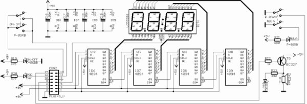
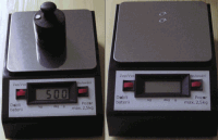
Now we will demonstrate by example what was said above. We will build a model that will work as a voltmeter with a digital scale. We agree that the maximum measured voltage will be 10V. Also let our layout display the contents of the ADC register on the LCD.
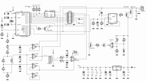
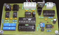
Connection diagram:

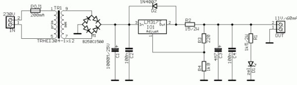
The binding of the microcontroller and LCD WH1602A is standard. X1 – a quartz resonator at 4 MHz, capacitors C1, C2 – 18-20 pF. The R1-C7chain at the reset pin is 10 kΩ and 0.1 μF, respectively. Signal LED D1 and limiting resistor R2 200 ohms and R3 – 20 ohms. LCD contrast adjustment – VR1 at 10 kΩ. The reference voltage source we will use is built in to 2.56V. With the help of the divider R4-R5 we will achieve the maximum voltage of 2.5V at the input of PC0 , with a voltage on the probe 10V. R4 – 3 kOhm, R5 – 1 kOhm, in their denomination should be treated carefully, but if it is not possible to choose exactly such, you can make any resistive 1: 4 divider and programmatically correct the readings, if necessary. A 10 μH choke and a 0.1 μF capacitor to eliminate noise and pickups on the ADC are not shown in the diagram. Their presence is implied if the ADC is used. Now it’s up to the program:

C program


#include 
#define RS 2 // RS = PD2
#define E 3 // E = PD3
#define TIME 10 // Time delay constant for LCD
// Frequency clocking MK - 4 MHz
#define R_division 3.837524 // = R4 / R5 constant
unsigned int u = 0 ; // Global variable with transform content
void pause ( unsigned int a )
{
unsigned int i ;
for ( i = a ; i > 0 ; i - ) ;
}
void lcd_com ( unsigned char lcd ) // Transmit LCD Command
{
unsigned char temp ;
temp = ( lcd & ~ ( 1 << RS ) ) | ( 1 << E ) ; // RS = 0 is a command
PORTD = temp ; // Output to the portD the top tetrad of the command, signals RS, E
asm ( "nop" ) ; // A small delay in 1 tact MK, to stabilize
PORTD = temp & ~ ( 1 << E ) ; // command recording signal
temp = ( ( lcd * 16 ) & ~ ( 1 << RS ) ) | ( 1 << E ) ; // RS = 0 is a command
PORTD = temp ; // Output the command, signals RS, E to portD
asm ( "nop" ) ; // A small delay in 1 tact MK, to stabilize
PORTD = temp & ~ ( 1 << E ) ; // command recording signal
pause ( 10 * TIME ) ; // Pause for command execution
}
void lcd_dat ( unsigned char lcd ) // Write data to LCD
{
unsigned char temp ;
temp = ( lcd | ( 1 << RS ) ) | ( 1 << E ) ; // RS = 1 is data
PORTD = temp ; // Output to the portD the highest data tetrad, RS, E signals
asm ( "nop" ) ; // A small delay in 1 tact MK, to stabilize
PORTD = temp & ~ ( 1 << E ) ; // Data Write Signal
temp = ( ( lcd * 16 ) | ( 1 << RS ) ) | ( 1 << E ) ; // RS = 1 is data
PORTD = temp ; // Display on the portD the lowest tetrad of data, signals RS, E
asm ( "nop" ) ; // A small delay in 1 tact MK, to stabilize
PORTD = temp & ~ ( 1 << E ) ; // Data Write Signal
pause ( TIME ) ; // Pause for data output
}
void lcd_init ( void ) // Initialize the LCD
{
lcd_com ( 0x2c ) ; // 4-wire interface, 5x8 character size
pause ( 100 * TIME ) ;
lcd_com ( 0x0c ) ; // Show image, do not show cursor
pause ( 100 * TIME ) ;
lcd_com ( 0x01 ) ; // Clear DDRAM and set the cursor to 0x00
pause ( 100 * TIME ) ;
}
unsigned int getADC ( void ) // Read ADC
{ unsigned int v ;
ADCSRA | = ( 1 << ADSC ) ; // Start conversion
while ( ( ADCSRA & _BV ( ADIF ) ) == 0x00 ) // Wait for the conversion to complete
;
v = ( ADCL | ADCH << 8 ) ;
return v ;
}
void write_data ( unsigned int u )
{ unsigned char i ;
double voltage = 0 ;
lcd_com ( 0x84 ) ; // Display the ADC register on the LCD
for ( i = 0 ; i < 10 ; i ++ )
if ( ( u & _BV ( 9 - i ) ) == 0x00 ) lcd_dat ( 0x30 ) ;
else lcd_dat ( 0x31 ) ;
lcd_com ( 0xc2 ) ;
voltage = R_division * 2.56 * u * 1.024 ; // Calculate Stress
i = voltage / 10,000 ; // Output Voltage On LCD
voltage = voltage - i * 10000 ;
if ( i ! = 0 ) lcd_dat ( 0x30 + i ) ;
i = voltage / 1000 ;
voltage = voltage - i * 1000 ;
lcd_dat ( 0x30 + i ) ;
lcd_dat ( ',' ) ;
i = voltage / 100 ;
voltage = voltage - i * 100 ;
lcd_dat ( 0x30 + i ) ;
i = voltage / 10 ;
voltage = voltage - i * 10 ;
lcd_dat ( 0x30 + i ) ;
lcd_dat ( 'v' ) ;
}
int main ( void )
{
DDRD = 0xfc ;
pause ( 3000 ) ; // Delay to turn on the LCD
lcd_init ( ) ; // Initialize LCD
lcd_dat ( 'A' ) ; // We write "ADC =" and "U =" on the LCD
lcd_dat ( 'D' ) ;
lcd_dat ( 'C' ) ;
lcd_dat ( '=' ) ;
lcd_com ( 0xc0 ) ;
lcd_dat ( 'U' ) ;
lcd_dat ( '=' ) ;
ADCSRA = ( 1 << ADEN ) | ( 1 << ADPS1 ) | ( 1 << ADPS0 ) ;
// Turn on the ADC, the clock frequency of the inverter = / 8 from the clock microcontroller
ADMUX = ( 1 << REFS1 ) | ( 1 << REFS0 ) | ( 0 << MUX0 ) | ( 0 << MUX1 ) | ( 0 << MUX2 ) | ( 0 << MUX3 ) ;
// Internal reference voltage source Vref = 2.56, the input of the ADC is PC0
while ( 1 )
{
u = getADC ( ) ; // Read data
write_data ( u ) ; // Display them on LCD
pause ( 30,000 ) ;
}
return 1 ;
}
The program is simple. At the beginning, we initialize the I / O ports. In order to serve as an input to the ADC , the pin PC0 must work as an input. Next, we carry out the initialization of the LCD and ADC . Initializing the ADC is to turn it on with the ADEN bit in the ADCSRA register.And the choice of frequency conversion bits ADPS2, ADPS1, ADPS0 in the same register. We also choose the reference voltage source, bitsREFS1 REFS0 in the ADMUX register and input of the ADC : bits MUX0, MUX1, MUX2, MUX3 (in our case, the input of the ADC is PC0 , therefore MUX0.3 = 0 ). Next, in the perpetual cycle, we start the conversion by setting the ADSC bit in the ADCSRA register. We are waiting for the conversion to finish (the ADIF to ADCSRA bit becomes 1). Next, remove the data from the register ADC and display them on the LCD . It is necessary to remove data from the ADC in the following sequence: v = (ADCL + ADCH * 256); if you use v = (ADCH * 256 + ADCL); - point blank does not work.

So there is a trick to not work with fractional numbers. When to calculate the input voltage in volts. We will simply store our voltages in millivolts.For example, the value of the voltage variable 4234 means that we have 4.234 volts. In general, operations with fractional numbers consume a lot of microcontroller memory (our voltmeter firmware weighs slightly more than 4 kilobytes, this is half the memory of ATmega8 programs!), They are recommended to be used only when absolutely necessary. Calculating the input voltage in millivolts is simple: voltage = R_division * 2.56 * u * 1.024;
Here R_division is the coefficient of the resistive divider R4-R5 . So, as the real divider coefficient can differ from the calculated one, our voltmeter will lie. But it’s easy to correct. Using a tester, we measure a certain voltage, we get X volts, and let our voltmeter show Y volts. Then R_division = 4 * X / Y , if Y is greater than X and 4 * Y / X if X is greater than Y. This completes the setting of the voltmeter, and it can be used.

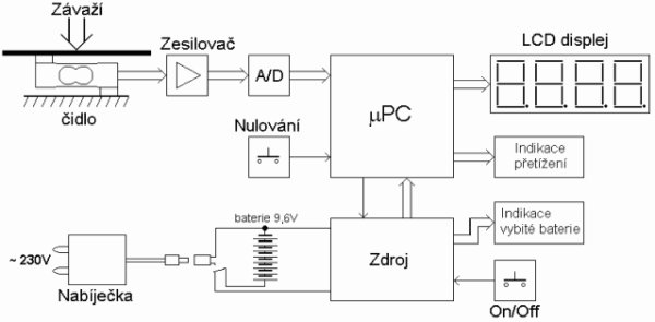
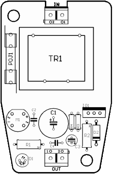
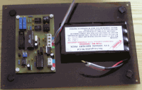
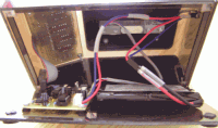
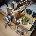
You can also modify your power supply. By inserting a digital voltmeter ammeter on the LCD and overload protection into it (to measure the current, we need a powerful shunt of about 1 Ohm resistance).
In my power supply, I also integrated the overload protection when the current exceeds 2A, then the piezo squeaker begins to squeak earnestly, signaling overload:

Source: avrlab.comz AVR Ammeter Volt Meter Project files Alternative link: adc-example-atmega8-digital-volt-meter-ammeter-project.rar

PROGRAMMED DOOR ALARM CIRCUIT ATTINY24 ATTINY13 CONTROLLED

$
0
0

This simple mini-burglar alarm on the ATtiny 13 microcontroller is designed to protect apartments, offices, summerDOOR ALARM CIRCUIT cottages … When the reed switch opens, the alarm beeps or, with a little refinement, you can send an SMS from a mobile phone. The alarm control is carried out by IR remote controls. Main features: dynamic power supply of the photo-receiver, wake-up from the “SLEEP” mode by interruption from the watchdog timer in the “POWER-DOWN” mode, and as a result low power consumption – about 30 μA.

The schematic diagram of the device is quite simple. IR receiver – TSOP1736. The heart of the device is the ATtiny13 microcontroller. When the reed switch contacts open, an alarm is triggered. Schematic diagram of the burglar alarm (click on the diagram to enlarge):

DOOR ALARM CIRCUIT schamatic

The assembled device looks like this:

DOOR ALARM CIRCUIT (1) DOOR ALARM CIRCUIT (2)

The infrared transmitter for controlling the alarm system is assembled on the ATtiny13 microcontroller and a dozen passive components. Instead of the BC847 transistor, you can use any low-power transistor, for example, a CT 315. The power source is two CR-type lithium-ion batteries. Schematic diagram of the infrared remote control to control the alarm system (installation of security / disarming):

DOOR ALARM CIRCUIT schamatic

Assembled keychain control:

DOOR ALARM CIRCUIT (3)

When using a multichannel (99 channel) IR transmitter on the ATtiny24 microcontroller, you can use a large number of nearby alarms at the same time, controlling them by choice. Schematic diagram of the multichannel IR transmitter:

DOOR ALARM CIRCUIT schamatic


Assembled multichannel IR transmitter:

DOOR ALARM CIRCUIT (4) DOOR ALARM CIRCUIT (5)


Alarm programming

Erasing all key chains

Set the jumper to JP1.
A beep will sound, the indicator continuously flashes in red 0.5 Hz

Adding new key chains

Set jumper on JP2.
The indicator flashes continuously in green 0.5 Hz.
In confirmation of the recording keychain beep beeps 1 time.
If the keyfob memory is full, the indicator continuously flashes red with 0.5 Hz.

Work with the device

Device status – disarmed (green LED flashes at 1 Hz)

Arming with the door closed

Press the button on the key fob for 1-2 seconds, directing it to the security device, a beep will sound 1 time.
The indicator flashes red with a frequency of 1 Hz.

Arming with the door open

Press the button on the key fob for 1-2 seconds, directing it to the security device, a beep will sound 1 time.
The indicator alternately flashes red and green with a frequency of 1 Hz.
After closing the door, the indicator flashes in red with a frequency of 1 Hz.

Disarm

Press the button on the key fob for 1-2 seconds, directing it to the security device, a beep will sound 2 times.
The indicator flashes green with a frequency of 1 Hz.

Alarm removal

Press the button on the key fob for 1-2 seconds, directing it to the security device, a beep will sound 2 times.
The indicator flashes green with a frequency of 1 Hz. After removing the alarm, if necessary, arm again.
source: radioded.ru All hex project, asm, bass have code files and schema drawings alternative link:programmed-door-alarm-circuit-attiny24-attiny13-controlled.rar

AT89C2051 DIGITAL SCALES CIRCUIT ATMEL

$
0
0

This is a kitchen scale with a maximum weight of 2.5kg and an accuracy of 10g. Exceeding the range is indicated by an acoustic signal and an LED. Weight is displayed on a four-digit LCD display. The weight also includes a weight-zero reset button. The power is solved by a battery whose discharge is below the set limit indicated by the LED.Then the battery needs to be recharged, otherwise the voltage drops below the operating level and the wrong weight information appears in the display. In order to avoid having to switch off the balance for unnecessary battery discharge, after 2 minutes of inactivity (only if there is no weight on the weight) it will turn itself off.

Block diagram :

Block diagram

Block diagram analysis: 
By weighing the weighing platform with force on the sensor, it deforms and at the same time changes the resistance of the 4 strain gauges attached thereto. These strain gauges are bridged. The output voltage of the sensor is of the order of magnitude, so it needs to be amplified for further processing, so I used the AD620 instrument amplifier. The amplification is set to 150. The amplified signal can now be converted to a digital value using the TLC549 8-bit serial A / D converter. The core of the full scale where the measured value is converted from the A / D converter to the correct weight reading displayed on the 4-digit LCD is the AT89C2051 μ-processor. If the weight is exceeded, the overload indicator is activated and —- appears on the display. The reset button is used to reset the current weight from which it will be read, for example: put the bowl on the scale and reset, only what we place on this bowl will be weighed. If we cut the bowl, —- will appear, we must reset the weight again, this time without a load. The balance is powered by a Ni-Cd battery that can be recharged if required by a built-in charger. When charging, the power for the rest of the balance is disconnected. The balance is switched on and off with the On / Off button (press on / off to turn off). To avoid unnecessary discharging of the battery, after 2 minutes of inactivity, the balance will turn off only if there is no weight on it. The low battery indication indicates that we should recharge the balance as soon as possible, otherwise weighing errors occur due to a low power supply, and incorrect weight information will be displayed on the display.

Control section diagram

Diagram of the imaging section
Diagram of the imaging section 

More detailed activity: 

Only IO4, transistor emitter T2, C11 and On / Off button are powered directly from the battery. Because the IO4 is made by CMOS technology, its take-off is minimal and hence the stand-by take-off of the whole balance when it is turned off. IO4 is connected as a T flip-flop (divider two). C11 and R14, after connecting the battery, sets output Q to log. H, the transistor T1 is closed, thereby interrupting the supply to the other part of the circuit. After pressing the button, CLK clock input is logged. H, the circuit is overturned, the transistors T1 and T2 are closed and the power balance of the rest of the balance is switched on. OZ3 is connected as a voltage comparator that monitors the battery voltage. If it drops below the set threshold by the trimmer P4, it switches on the transistor T3, which has an LED indicator in its collector and indicates a weak battery. For other circuits, we need a voltage + 5V, which is obtained from the IO5 stabilizer, C12 – C14 only serves to filter the voltage. The strain gauge sensing sensor is in the bridging circuit and at its output is a signal in the order of mV. This signal is too small for further processing, so integrated IC amplifier IO2 is connected to the circuit, its gain is 150 and is given by the Trimmer P3, which is set to 330. The amplified signal is further superimposed on the constant voltage (approximately 1 , 0 V), this is obtained from a multiple voltage divider and impedantly separated by the OZ2A operational amplifier. This amplified signal is applied to the A / D input IO3 converter. The range of the converter can be set by bringing two reference values to its REF + (about 2.7V) and REF- (about 1.1V) inputs. Both voltages are derived from the same voltage divider and impeded by OZ1. The size of the reference values can be set by the P1 and P2 trimmers to determine the lower and upper limits for the converter. According to the converter manufacturer, the difference between the reference values must always be greater than 1V. The amplified and converted signal is processed by the IO1 processor (more). The processor is in standard wiring, the C9 and R8 components ensure that when the processor reset is turned on, the Q1 crystal taps it at 24MHz.Output from the processor goes through the four 8-bit IO6-IO9 sliding registers that drive DIS1 segments on the LCD display. The common display terminal is connected directly to the processor port. Display segments need to be triggered by an AC signal with a frequency of 20 to 150 Hz (40 to 300x / s change). This means that the common outlet is set to the log. H and display the segments displayed in the log. L and vice versa the next time you broadcast. If the 2.5kg weight is exceeded (regardless of possible reset), the processor switches the transistor T5 and starts the piezo-siren SIR and the DSIR LED indicating overload. When the zero key is pressed, the processor port P3.2 is grounded, which is the input of the external interrupt and the processor remembers the current weight on the scale. If no weight is placed on the weight and is idle for 2 minutes, the transistor T4 switches on, which transmits the IO4 log to the CLK input. H, it flips and interrupts the power supply for the processor and other components except IO4. Weighing in operation is about 40mA.

Design of printed circuit boards – control:

Upper side – staff:
Upper side - staff

Bottom side – toolbar:
Bottom side - toolbar

Design of printed circuit board (90 x 57 mm). 

Design of printed circuit board


Design of PCB – Display:

Upper side – staff:
Upper side - staff

Design of printed circuit board (104 x 56 mm).
Design of printed circuit board
Design of printed circuit board (1)


Program function analysis

Program function analysis: 

After resetting the processor, the values are initialized and a timer 0 is started, which determines when to be sent to the display and timer 1, which determines when the new value from the A / D converter should be read. After setting, the value from the converter is read and the program starts. First, read from the read value is the value stored at zero (currently 0) and compares if it is not in negative values when it is displayed on the display —-. If it does not find out if the weight is zero, then it starts counting for 2 minutes, which turns off if the zero weight is not changed. Now it compares the value of the A / D converter to see if the weight of 2.5kg is exceeded, otherwise the overload indication will be switched on. It also uses a division to find thousands, hundreds, tens, and units. If there is something else 0, it compares the others and excess zeros are not displayed on the display. The number of thousands, hundreds, tens and units needs to be converted to a combination of bits to display the desired number on the display. The weight data is processed and ready for broadcasting, so the program detects whether it has already timed out and does not transmit on the display, otherwise it compares if the new value of the A / D converter should not be read, if not compare the transmission to the display. .
The program has about 300 lines and you can download it here – it’s complete with a lot of comments.


Scheme, design and charger description :

This is a simple charging connection for a Ni-Cd battery. This connection is not the most appropriate, but it is sufficient for occasional charging. I’ve chosen this simple connection to get the charger into the U-KPZ3 adapter box. The mains voltage is fed via a fuse to a transformer with a secondary voltage of 12V. This voltage is thrust across the M1 bridge, filtered through C1, C2 and applied to the LM317T regulated voltage stabilizer. With the R3 and R4 resistors the output voltage is set to 11.5V according to the formula U out = 1.25 (1 + R4 / R3). By R2, a constant charging current is set to 60 mA according to the formula I out = 1,25 / R2. This strain is filtered using C3, C4. The D1 LED serves only to indicate that the charger is on the network. The D2 protects the stabilizer against back-up by disabling the charger before disconnecting the rechargeable battery. It is advisable to place a small cooler on the IO1. The Ni-Cd battery is about to charge about 125% of the battery voltage, which in my case is 12V and current approximately 1/10 of the battery capacity, that is 60mA. I deliberately lowered the charging voltage to avoid potential battery damage.

Charger connection diagram:
Charger connection diagram

Design of printed circuit boards (48.5 x 75 mm) and layout of components:

Design of printed circuit boards (48.5 x 75 mm) and layout (2) Design of printed circuit boards (48.5 x 75 mm) and layout (1)


List of used components:
  C1 100n
  C2, C3 22p - 2x
  C4-C8, C10, C12,
  C13, C15 - C19 100n - 13x
  C9 22M / 16V
  C11, C14 10M / 25V - 2x

  R1 1k8
  R2 - R4, R6, R7,
  R9, R15, R18, R22 1k - 9x
  R16 1k SMD 1206
  R5 560
  R8 5k6 SMD 1206
  R10 - R12 4k7 mini - 3x
  R13, R14, R17 10k - 3x
  R19 1k5
  R20 1k2
  R21 680
  R23 390
  P1, P2 PM19K001 - 2x
  P3 PM19E500
  P4 PT-6VK005

  DZ1 BZX83V056
  DZ2 BZX83V033
  T1 BC560
  T2 BD140
  T3 BC546
  T4 BC556
  T5 BC327

  IO1 AT89C2051
  IO2 AD620
  IO3 TLC549
  IO4 4013
  IO5 78L05
  IO6 - IO9 4094 - 4x
  OZ1, OZ2 LM358 - 2x
  OZ3 TL071
  Q1 24MHz
 DIS1 LCD3906
 DSIR LED 3mm red
 POD LED 3mm red

 Strain gauge DF2S-3 / 5kg
 ZERO, ON / OFF P-0SRB - 2x
 SIR KPE242
 BAT ARK500 / 2
 CIDLO ARK500 / 2 - 2x
 CON1, CON2 MLW14G - 2x
 PFL14 connectors - 2x
 flat cable AWG28-14 (15cm)
 B-8F600AA battery
 power connector K3716A
 display frame AR1950


 Charger :
 C1 1000M / 25V
 C2, C4 100n - 2x
 C3 4M7 / 50V

 R1 1k5 / 2W
 R2 15 / 2W
 R3 220
 R4 1k8

 D1 LED 3mm green
 D2 1N4007
 IO1 LM317T
 M1 B250C1500
 TR1 TRHEI304-1x12

 IN, OUT ARK500 / 2 - 2x
 POJ1 KS20-01 footrest
 tube fuse 200mA

 adapter box U-KZ3
 power connector SCP-2009B
 cable to connect the charger to the balance


Finally some photos completed and FUNCTIONAL scales. Finally some photos completed and FUNCTIONAL scales (1) Finally some photos completed and FUNCTIONAL scales (2) Finally some photos completed and FUNCTIONAL scales (3) Finally some photos completed and FUNCTIONAL scales (4)

Source: http://paja-trb.unas.cz/elektronika/konstrukce/vaha.html Digital Scales project Alternative link:at89c2051-digital-scales-circuit-atmel.RAR


ATMEGA128 AVR GRAPHIC LCD APPLICATION SIEMENS S65 LS020

$
0
0

Siemens s65 using the Atmel ATmega128 caption to display graphics on the LCD all the resources an application prepared S65 LCD driver library, sample text and detailed graphics shared C code. S65 application is… Electronics Projects, ATmega128 AVR Graphic LCD Application Siemens S65 LS020 “avr project, microcontroller projects, “

GRAPHIC LCD APPLICATION

Siemens s65 using the Atmel ATmega128 caption to display graphics on the LCD all the resources an application prepared S65 LCD driver library, sample text and detailed graphics shared C code.

S65 application is more complex graphic LCD (given schematic diagram) is connected to the microcontroller ATmega128 directly behind the LCD not LCD 2.9-volt power supply and a few passive components oscillator is staying placement.

ATMEL ATMEGA128 SIEMENS S65 (1) ATMEL ATMEGA128 SIEMENS S65 (2)

The S65-Display is a 132x176x65536 color display. display use a slave SPI communication controller is unknown and can be used with an SPI clock up to 13 MHz. The software was used with an ATmega128 at 8MHz SPI clock.

Source: S65-Display-Software AVR Graphic LCD Alternative link: atmega128-avr-graphic-lcd-application-siemens-s65-ls020.rar

ATMEGA16 TOUCHSCREEN PROJECT TFT APP AVR GCC ILI9325

$
0
0

Touch TFT application based on ATMega16 processor used in the 16 MHz frequency drives and ILI9325 OTM3225, source C code (AVR GCC)’s. Source: ourdev.cn 2.4-inch TFT LCD, point-screen work notes Alternative link: atmega16-touchscreen-project-tft-app-avr-gcc-ili9325.rar… Electronics Projects,Atmega16 Touchscreen Project TFT App AVR GCC ILI9325 “avr project, microcontroller projects, “

TOUCHSCREEN PROJECT

Touch TFT application based on ATMega16 processor used in the 16 MHz frequency drives and ILI9325 OTM3225, source C code (AVR GCC)’s.

TOUCHSCREEN PROJECT(1)

Source: ourdev.cn 2.4-inch TFT LCD, point-screen work notes Alternative link: atmega16-touchscreen-project-tft-app-avr-gcc-ili9325.rar

TFT LCD DIGITAL PHOTO FRAME ATMEGA128 SD CARD TSC2046

$
0
0

Digital Photo Frame TFT ATmega128 TFT source C code of practice are used to SPFD5408 TFT LCD 3.2 inch 320 × 240 size images displayed in the SD card. Source: ourdev.cn/ Digital Photo Frame… Electronics Projects, TFT LCD Digital Photo Frame ATmega128 SD Card TSC2046 “avr project, microcontroller projects, “

LCD DIGITAL PHOTO FRAME

Digital Photo Frame TFT ATmega128 TFT source C code of practice are used to SPFD5408 TFT LCD 3.2 inch 320 × 240 size images displayed in the SD card.

LCD DIGITAL PHOTO FRAME (1)

Source: ourdev.cn/ Digital Photo Frame project Alternative link: tft-lcd-digital-photo-frame-atmega128-sd-card-tsc2046.RAR alternative link2 alternative link2

TFT LCD OV7660 ATMEL ATMEGA32 APPLICATION EXAMPLE ILI9325 DRIVER

$
0
0

Emerging technologies on the market with LCD prices quite fell microcontrollers with applications proliferate mobile phone, mp4 and graphic LCDs became available, especially Atmel series with enhanced graphics LCDs can be used ATmega32 320… Electronics Projects, TFT LCD OV7660 Atmel ATmega32 Application Example ili9325 Driver “avr project, microcontroller projects, “

LCD OV7660 ATMEL ATMEGA32 APPLICATION

Emerging technologies on the market with LCD prices quite fell microcontrollers with applications proliferate mobile phone, mp4 and graphic LCDs became available, especially Atmel series with enhanced graphics LCDs can be used ATmega32 320 × 240 TFT LCD application library files (ILI9325.H, ILI9325.C, font. h) includes the C source code and circuit diagram. In addition, the project “ov7660” camera that used a lot of cameras used in mobile phone, mp4 player, a tiny camera in the overall system implementation for different projects can inspire ..

ATMEGA32 OV7660 TFT EXAMPLE ILI9325

ATMEGA32 OV7660 TFT EXAMPLE ILI9325

Source: goo.gl/XbrE ATmega32 ili9325 Driver OV7660 alternative: tft-lcd-ov7660-atmel-atmega32-application-example-ili9325-driver.rar

ATMEL ATMEGA8 NOKIA6100 LCD PCF-8833 APPLICATION

$
0
0

Nokia 3310 screen already had several applications with bi-color LCD at this time I decided to experiment with it. Heavily on the market, the Nokia 6100 LCDs and their controllers for microchip using Atmel…Electronics Projects, Atmel Atmega8 Nokia6100 LCD PCF-8833 Application “atmega8 projects, avr project, microcontroller projects, “

NOKIA6100 LCD PCF-8833 APPLICATION

Nokia 3310 screen already had several applications with bi-color LCD at this time I decided to experiment with it. Heavily on the market, the Nokia 6100 LCDs and their controllers for microchip using Atmel ATmega8 given codes can edit and work with Winavi made to optimize and tried with ATmega8 code works just fine.

220Ω, and 330Ω with ATmega8 voltage divider screen I used to drive. But who wants to run ATMega8 3.3 volts without the use of resistance can take the screen. Including 8-bit and 12-bit color display mode has two 8bit color I did with trials. Drivers in the file by writing to the screen, draw various geometric shapes and functions available in press bmp image. All the files associated with the application can be accessed from the link below.

ATMEGA8 PCF8833 NOKIA 6100 PROJECT

ATMEGA8 PCF8833 NOKIA 6100 PROJECT schamatic

Atmega-8 Nokia 6100 lcd pcf-8833 application source code : https://320volt.com/en/atmel-atmega8-nokia-6100-lcd-pcf8833-uygulamasi/ and the circuit diagram: atmel-atmega8-nokia6100-lcd-pcf-8833-application.ZIP

Viewing all 1082 articles
Browse latest View live